
Makeup
Identifying Fake Small-Signal Transistors
Aug
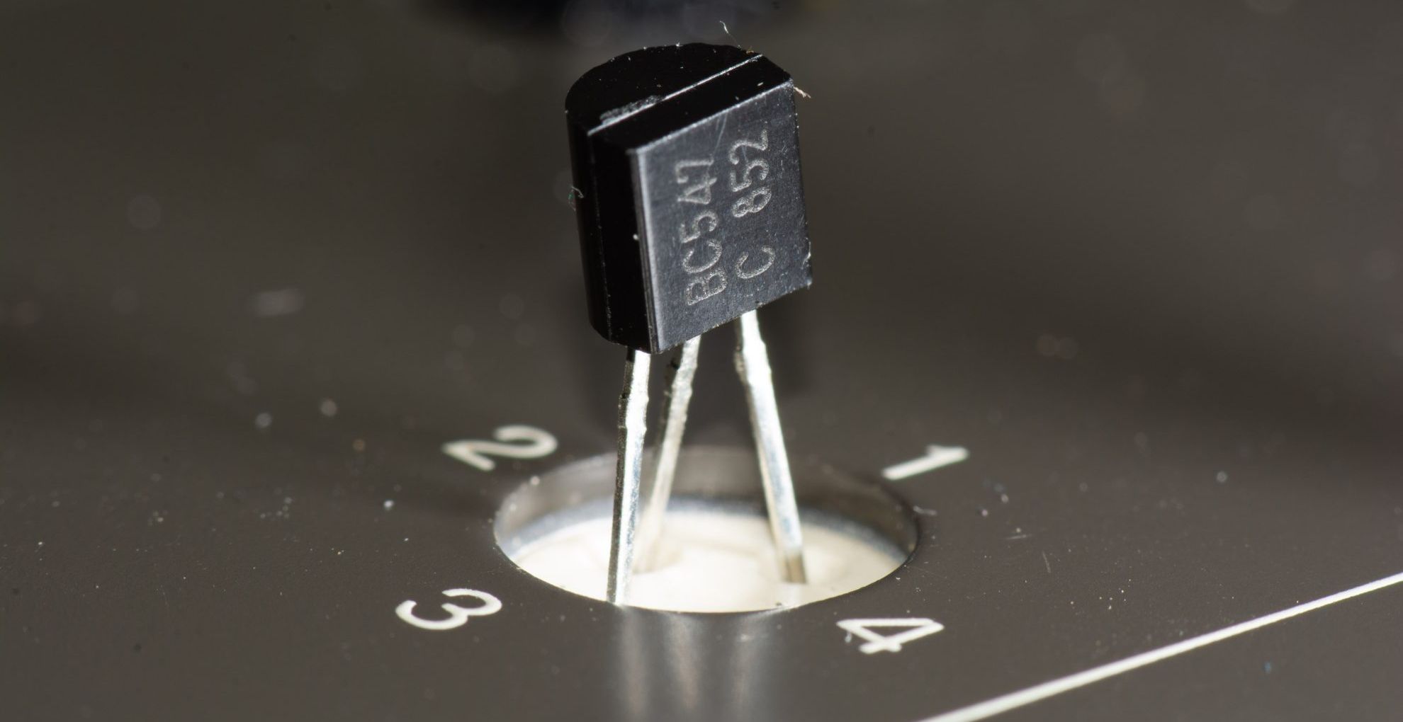
A fake small-signal transistor rarely arrives wearing a tiny villain mustache. It usually looks perfectly ordinary: a black plastic package, three shiny leads, and a familiar part number such as 2N3904, 2N2222A, BC547, or BC557. It may even pass a quick multimeter test. Then it enters a real circuit, where the gain collapses, leakage climbs, switching becomes sluggish, or the device fails at a fraction of its advertised voltage.
Counterfeit transistors include more than freshly manufactured copies. Some are recovered from discarded circuit boards, cleaned, resurfaced, and marked as new. Others are lower-grade devices relabeled as faster, quieter, higher-voltage, or more valuable parts. A few are genuine but aged, damaged, improperly stored, or represented with false date and lot codes. The package may be convincing while the silicon inside tells an entirely different story.
Fortunately, identifying fake small-signal transistors does not always require a laboratory full of equipment. Careful sourcing, visual inspection, comparison testing, and a handful of well-chosen electrical measurements can expose many impostors before they become permanent residents of your circuit board.
Why Small-Signal Transistors Are Counterfeited
Individual general-purpose transistors are inexpensive, but they are sold in enormous quantities and used in amplifiers, oscillators, sensor interfaces, switching stages, protection circuits, and industrial repairs. Obsolete or temporarily unavailable versions may command much higher prices than common current-production parts.
The economics become attractive to counterfeiters when a buyer needs thousands of devices, an exact vintage part number, a particular gain grade, or a discontinued package. Reclaimed parts can be removed from scrap boards, straightened, cleaned, recoated, and printed with a desirable marking. A cheaper transistor can also be relabeled as a premium low-noise or high-frequency model.
The result may function well enough to survive a basic continuity test. Reliability, parameter stability, and performance at voltage, current, frequency, or temperature extremes are another matter. Semiconductor manufacturers warn that products obtained outside authorized channels may be counterfeit, modified, improperly handled, beyond recommended storage periods, or unsupported by the original manufacturer.
Begin with the Supply Chain
Buy from an authorized source whenever possible
The most effective counterfeit test happens before the package is opened: purchase from the original component manufacturer or an authorized distributor. Authorized distributors maintain manufacturer relationships, traceability records, quality systems, and controlled return procedures. Industry standards such as SAE AS6496 establish counterfeit-mitigation requirements for authorized distribution.
Marketplace sellers, anonymous brokers, auction listings, and surplus dealers are not automatically dishonest. They simply create a higher-risk transaction because traceability may end at the seller’s keyboard. When a component is readily available through authorized channels but an unknown vendor offers it at one-tenth the normal price, the discount is not necessarily a miracle. Sometimes it is an electrical practical joke with shipping included.
Check the paperwork and listing
Before testing the devices, save the invoice, listing photographs, packaging labels, seller claims, and stated manufacturer. Ask for the full manufacturer part number, country of origin, date code, lot information, and a certificate of conformance when the application justifies it.
Warning signs include:
- A price dramatically below normal authorized-distributor pricing
- Large quantities of a supposedly scarce or discontinued transistor
- Generic bags without manufacturer labels or traceability
- Mixed date codes presented as one factory lot
- Labels placed over older labels
- Spelling errors, distorted logos, or inconsistent part-number formatting
- A seller who avoids identifying the actual manufacturer
Packaging alone cannot authenticate a transistor, but poor packaging can quickly establish that additional inspection is necessary.
Perform a Careful Visual Inspection
Use magnification and good lighting
Examine the parts under bright, angled light with a loupe or low-power microscope. Professional counterfeit-screening procedures commonly begin with documented external visual inspection before progressing to more expensive tests. A known genuine sample from the same manufacturer and package generation is especially valuable because logos, fonts, molds, and marking methods legitimately change over time.
Do not compare a modern onsemi TO-92 package with a thirty-year-old Motorola device and declare one fake because the typography differs. Compare like with like: manufacturer, part number, package style, approximate production period, and preferably ordering suffix.
Inspect the printed markings
Look for uneven character spacing, blurry printing, crooked lines, incorrect logos, inconsistent font weight, or characters that vary among devices supposedly taken from one lot. Check whether the date-code format agrees with the manufacturer’s documented marking system.
For example, an onsemi 2N3904 data sheet shows a specific TO-92 marking format that includes the device identifier and year-and-work-week information. It also documents the terminal arrangement and package details. The correct reference is always the data sheet for the claimed manufacturer, not a random pinout graphic found in an online forum.
Look for resurfacing and remarking
Reclaimed parts may be sanded to remove the original text and then covered with a dark coating commonly called blacktop. Under angled light, the top surface may show a different texture, gloss, or color from the sides. Rounded package edges may appear flattened, mold marks may be partially filled, or the printed area may look unusually smooth.
A solvent-based marking-permanency test can sometimes reveal an added coating or weak replacement ink, but it is not a universal authenticity test. Genuine marking systems vary, and aggressive solvents can produce false conclusions or damage legitimate parts. Professional guidance treats surface testing as one element of a broader inspection sequence, not as a magic cotton swab of truth.
Examine the leads
New through-hole transistor leads should generally be consistent in shape, finish, spacing, and length for a given packaging method. Suspicious clues include scratches near the body, residual solder, uneven tinning, flattened sections, heavy oxidation, bent-and-restraightened leads, or tiny impressions left by removal tools.
These signs may indicate reclamation, but they do not always prove counterfeiting. Genuine old stock can have oxidized leads, and parts repackaged by an authorized service may have legitimate variations. The correct conclusion may be “aged or nonconforming” rather than “counterfeit.” Both categories can still be unsuitable for production.
Measure the package
Use calipers to compare body width, height, thickness, lead spacing, and lead diameter with the manufacturer’s package drawing. Significant dimensional discrepancies are suspicious, particularly when combined with marking or surface anomalies. Professional inspection methods use package configuration and dimensional analysis because a relabeled device may come from a different mold family.
Test the Junctions with a Digital Multimeter
A bipolar junction transistor contains two semiconductor junctions sharing the base terminal. A multimeter in diode mode can identify transistor polarity, locate the base, detect open junctions, and reveal some incorrectly marked or badly damaged devices.
Testing an NPN transistor
- Place the red probe on the suspected base.
- Touch the black probe to the other two leads individually.
- A healthy silicon device will commonly show a forward drop in the general neighborhood of 0.55 to 0.75 volts for both junctions.
- Reverse the probes. Both junctions should normally read open at the meter’s test voltage.
- Measure between collector and emitter in both directions. With the base unconnected, the meter should normally indicate no ordinary diode conduction.
Testing a PNP transistor
The process is reversed. Place the black probe on the base and touch the red probe to the emitter and collector. Both junctions should conduct in that direction and block when the probes are reversed.
A diode-mode test is useful, but it does not establish authenticity. A cheap substitute transistor and a genuine premium transistor may display nearly identical junction drops. Temperature, test current, semiconductor process, and meter design also influence the reading.
Confirm the Pinout Instead of Guessing
Do not assume every TO-92 transistor uses the same emitter-base-collector arrangement. Devices with similar names may use different pinouts, and the orientation can change with manufacturer, package suffix, or regional naming convention.
After locating the base with diode mode, distinguish collector from emitter by comparing gain in both orientations or by building a low-current test circuit. A bipolar transistor usually operates with noticeably higher gain when collector and emitter are connected correctly. Reverse operation may still produce current, which is why a quick test can occasionally fool the unwary.
A pinout mismatch is not proof of counterfeiting until the exact manufacturer data sheet has been checked. Many innocent transistors have been accused because someone consulted a diagram for a different brand.
Measure Current Gain Under Controlled Conditions
The hFE socket on a handheld multimeter is convenient for sorting parts, but its test conditions may not match the data sheet. Current gain changes with collector current, collector-emitter voltage, temperature, and individual production variation. A single unexplained beta number is therefore weak evidence.
A better test uses a current-limited bench supply, measured base current, and measured collector current:
DC current gain, hFE = collector current divided by base current.
Set the transistor to the collector current and collector-emitter voltage specified in the data sheet. Measure several samples from the suspect lot and compare them with a known genuine device under identical conditions.
As a concrete example, the onsemi 2N3904 specification lists DC gain limits at several operating points. At a collector current of 10 mA and a collector-emitter voltage of 1 V, the listed hFE range is 100 to 300. At higher collector current, the guaranteed minimum changes. That is why testing only at a tiny current can allow a wrongly relabeled device to appear acceptable.
Test at two or three useful current levels. A suspicious device may show respectable gain at 100 microamps but collapse at 10 or 50 mA. A genuine transistor may also have gain near the low end of the allowed range, so compare measurements with published limits rather than personal expectations.
Check Collector-Emitter Saturation Voltage
For switching applications, collector-emitter saturation voltage is often more revealing than unloaded gain. Drive the transistor with a defined base current, pass a defined collector current, and measure the voltage from collector to emitter.
The onsemi 2N3904 data sheet, for example, specifies a maximum VCE(sat) of 0.2 V at 10 mA collector current with 1 mA base current. At 50 mA collector current and 5 mA base current, the maximum is 0.3 V. These are forced-beta conditions of ten, not measurements made with the base barely tickled through an enormous resistor.
A substitute die may pass diode and low-current gain tests yet produce excessive saturation voltage. That can cause dim LEDs, weak relay drive, excess heating, incorrect logic levels, or intermittent operation in circuits designed with limited voltage headroom.
Measure Leakage and Breakdown Carefully
Collector leakage is frequently overlooked because an ordinary multimeter cannot resolve very small currents reliably. A semiconductor analyzer, source-measure unit, or carefully designed guarded test fixture may be required for nanoamp-level measurements.
Leakage that is substantially higher than the data-sheet limit can indicate damage, contamination, aging, an incorrect die, or a counterfeit part. Measure multiple devices and allow readings to stabilize, since fingerprints, humid circuit boards, and dirty fixtures can create leakage paths larger than the transistor current being measured.
Breakdown testing can reveal a lower-voltage transistor hidden under a higher-voltage marking. It must be performed with strict current limiting and suitable equipment. A curve tracer applies voltage while monitoring collector current, allowing the breakdown knee to be compared with the specified minimum. Tektronix guidance describes collector-emitter breakdown testing with the base open and collector current monitored as voltage rises.
Do not casually connect a transistor to a high-voltage supply and wait for drama. Exceeding ratings or allowing excessive current can permanently alter or destroy the sample. For inexpensive transistors, replacing the lot from an authorized source is often safer and cheaper than improvised breakdown testing.
Test Capacitance, Speed, and Noise When They Matter
Counterfeit devices can pass static DC tests while failing in high-frequency or low-noise applications. Junction capacitance, transition frequency, switching time, and noise performance depend strongly on die geometry and fabrication process.
For the onsemi 2N3904, the published characteristics include output capacitance, input capacitance, gain-bandwidth product, switching times, and noise figure under defined conditions. Measuring all of these at home is unnecessary, but one or two application-relevant dynamic tests can be valuable.
An LCR meter can compare junction capacitance across a sample group. A simple common-emitter amplifier can reveal unexpected high-frequency roll-off. A switching fixture with an oscilloscope can compare rise, fall, and storage times. For low-noise transistor grades, a real noise measurement is far more meaningful than a printed suffix on the package.
Use Lot-Level Comparison, Not a Single Heroic Sample
Counterfeit lots are often inconsistent. One bag may contain several die types, reclaimed parts from different years, or a mixture of genuine and substituted devices. Testing one unit and declaring victory is like inspecting one French fry and certifying the entire restaurant.
Sample devices from different positions in the bag, tube, or reel. Record:
- Package dimensions and weight
- Base-emitter voltage at a defined current
- Current gain at several collector currents
- Saturation voltage
- Leakage, where measurable
- Capacitance or switching behavior when relevant
Compare the distribution with a known-good lot. A broad or bimodal set of measurements can indicate mixed devices. Extremely uniform measurements are not automatically suspicious because factory lots and gain-binned parts can be tightly grouped. The important question is whether the behavior is plausible, internally consistent, and within the manufacturer’s limits.
When Professional Analysis Is Justified
High-reliability industries use progressively stronger methods according to supplier risk, application risk, and the value of the lot. Available techniques include X-ray imaging, X-ray fluorescence, scanning acoustic microscopy, scanning electron microscopy, material analysis, electrical characterization, and destructive decapsulation.
X-ray imaging can compare die size, die position, and bond-wire structure with a genuine reference. XRF can analyze lead finish and material composition. Decapsulation exposes the die so that logos, geometry, bond pads, and manufacturing details can be examined directly. Industry and government guidance treats these methods as parts of a risk-based test sequence rather than relying on one universal test.
Professional testing makes sense when the lot is valuable, the device is obsolete, replacement is impossible, or failure could create safety, regulatory, financial, or mission consequences. For a bag of common 2N3904 transistors intended for hobby projects, ordering verified replacements is normally the rational engineering decision.
A Practical Screening Workflow
- Verify the seller. Determine whether the source is manufacturer-authorized and whether traceability exists.
- Preserve evidence. Save labels, invoices, photographs, and seller claims before opening or mixing the lot.
- Obtain the correct data sheet. Match the claimed manufacturer, full part number, package, and suffix.
- Inspect the entire lot. Look for mixed markings, resurfacing, damaged leads, inconsistent molds, and packaging anomalies.
- Confirm polarity and pinout. Use diode mode and compare the result with the manufacturer documentation.
- Run controlled DC tests. Measure gain at multiple currents and check saturation voltage under specified conditions.
- Add application-specific testing. Measure leakage, capacitance, switching speed, breakdown, or noise when those parameters matter.
- Compare with a golden sample. Test a known genuine device in the same fixture whenever possible.
- Quarantine suspicious stock. Do not mix questionable parts with approved inventory or install them in customer products.
- Escalate or replace. Use a qualified laboratory for high-consequence applications; otherwise, replace the lot through an authorized source.
Common Mistakes That Produce False Accusations
Calling every low-gain transistor fake
Current gain naturally varies. A device near the specified minimum can be genuine and fully compliant. Test under the correct data-sheet conditions before reaching a conclusion.
Assuming all packages share one pinout
Similar-looking transistors can use different lead arrangements. Even a perfectly authentic component will behave badly when installed backward.
Treating a solvent test as final proof
Marking and molding technologies vary. A surface that reacts unexpectedly may justify more inspection, but it does not identify the die inside.
Ignoring storage and handling damage
A transistor may be genuine but degraded by electrostatic discharge, moisture, corrosion, excessive heat, or rough removal from old equipment. Authenticity and fitness for use are related but separate questions.
Testing only one operating point
A relabeled device may imitate the desired transistor at low current and room temperature. Differences often become obvious at higher current, elevated voltage, increased frequency, or temperature extremes.
Bench Experience: What Usually Exposes the Pretenders
Practical inspection experience teaches one lesson quickly: the most suspicious-looking transistor is not always the worst one. Some reclaimed components are crudely sanded, heavily recoated, and printed with lettering that appears to have been applied during a small earthquake. Those are easy. The difficult devices are clean, consistent, and electrically believable at first glance.
A common example involves a bag of supposed 2N3904 transistors that passes the multimeter diode test perfectly. Both junctions show reasonable forward voltage, collector-to-emitter conduction appears absent, and the meter’s hFE socket reports values around 180. Everything seems cheerful. When the devices are tested at a collector current of 10 mA, however, the sample divides into two groups. One group maintains expected gain and low saturation voltage. The other loses gain rapidly and shows a VCE(sat) several times higher than expected. The bag probably contains mixed die, reclaimed devices, or a substitute transistor sold under one marking.
Another recurring experience is the “wrong pinout panic.” A technician installs a BC547 where a 2N3904 had been used, assumes the flat-faced TO-92 packages are wired identically, and obtains nonsense readings. The replacement is condemned as fake before anyone checks the data sheets. Rotating the part or correcting the board footprint solves the mystery. The lesson is wonderfully unglamorous: verify the manufacturer’s pinout before beginning a criminal investigation.
Visual uniformity can also be misleading. In one lot, every package may have sharp printing and identical surfaces, yet electrical measurements reveal two distinct capacitance or gain populations. In another lot, printing varies slightly while all measured parameters remain consistent because the manufacturer used more than one legitimate assembly site or marking machine. Appearance is evidence, not a verdict.
Old stock creates a different puzzle. Leads may be dull, oxidized, or difficult to solder, but the transistors can still be genuine. Conversely, freshly tinned leads may hide reclaimed parts whose original solder and corrosion were removed. A solderability problem identifies a manufacturing risk, not necessarily a counterfeit. This distinction matters in professional purchasing because “genuine,” “new,” “unused,” and “suitable for production” are not interchangeable promises.
The strongest bench results usually come from comparison fixtures. Place a known genuine transistor and a suspect transistor into the same socket, use the same supply, allow the same warm-up time, and repeat the same measurements. Compare gain at 100 microamps, 1 mA, 10 mA, and perhaps 50 mA when the rating permits. Then compare saturation voltage and switching behavior. Absolute measurements are useful, but side-by-side curves often make a wrong die obvious without requiring heroic precision.
Temperature can expose additional differences. Warm both samples moderately and safely, then repeat leakage and gain measurements. Leakage normally rises with temperature, but a damaged or unsuitable transistor may increase far more dramatically. This does not prove fraudulent marking by itself; it shows that the part does not behave like the reference and may be unreliable in the intended circuit.
The final practical lesson is economic. Engineers sometimes spend an entire afternoon proving that a five-dollar bag of transistors is questionable. The investigation is educational, but it is not always efficient. When verified replacements are readily available, buying a fresh lot from an authorized distributor is usually cheaper than characterizing every mystery component. Save advanced testing for obsolete parts, expensive inventories, failure analysis, or situations in which the consequences justify the effort.
Conclusion
Identifying fake small-signal transistors requires more than reading a part number or checking two diode junctions. Begin with supplier traceability, compare packaging and markings with the correct manufacturer documentation, inspect the leads and body, and measure electrical parameters under defined data-sheet conditions.
The most useful affordable tests are polarity and pinout verification, current gain at multiple collector currents, and collector-emitter saturation voltage. Leakage, breakdown, capacitance, switching speed, and noise measurements provide stronger evidence when the application demands them. Whenever possible, compare the suspect lot with a known genuine sample.
No single clue proves that a transistor is counterfeit. A blurry logo may be harmless, while a beautiful package may conceal the wrong silicon. Confidence comes from combining provenance, visual evidence, repeatable electrical measurements, and application-specific testing. In electronics, as in detective stories, the quiet details usually catch the culprit.
Note: This article provides a practical screening workflow rather than formal authentication. Use current limiting, ESD controls, appropriate voltage-rated equipment, and qualified laboratories for destructive testing or safety-critical applications. The technical guidance was synthesized from semiconductor manufacturers, authorized distributors, electronics-industry organizations, test-equipment documentation, and U.S. government counterfeit-parts resources.

